Introduction
ATC0 (ASSAM Test Chip 0) is the first test chip designed by the SCALE group at MIT. It serves the purpose of debugging the design process, tool chain flow, testing strategies for future hardware modules, and characterizing the fabrication process. ATC0 also implements an interface between itself and an external controller which will be used for the series of future Pekoe chips. ATC0 will be fabricated in a 0.18 micron CMOS process with six aluminum metal layers from TSMC, sized at 2.7mm x 2.7mm.For more information see the design document.
Photos
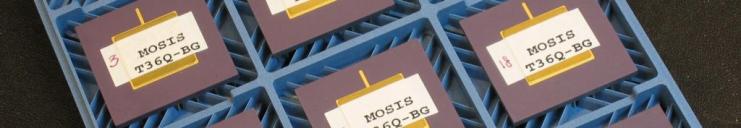
We received 20 packaged chips from Mosis...
...and we pried one open for a die photo (click for a larger view).

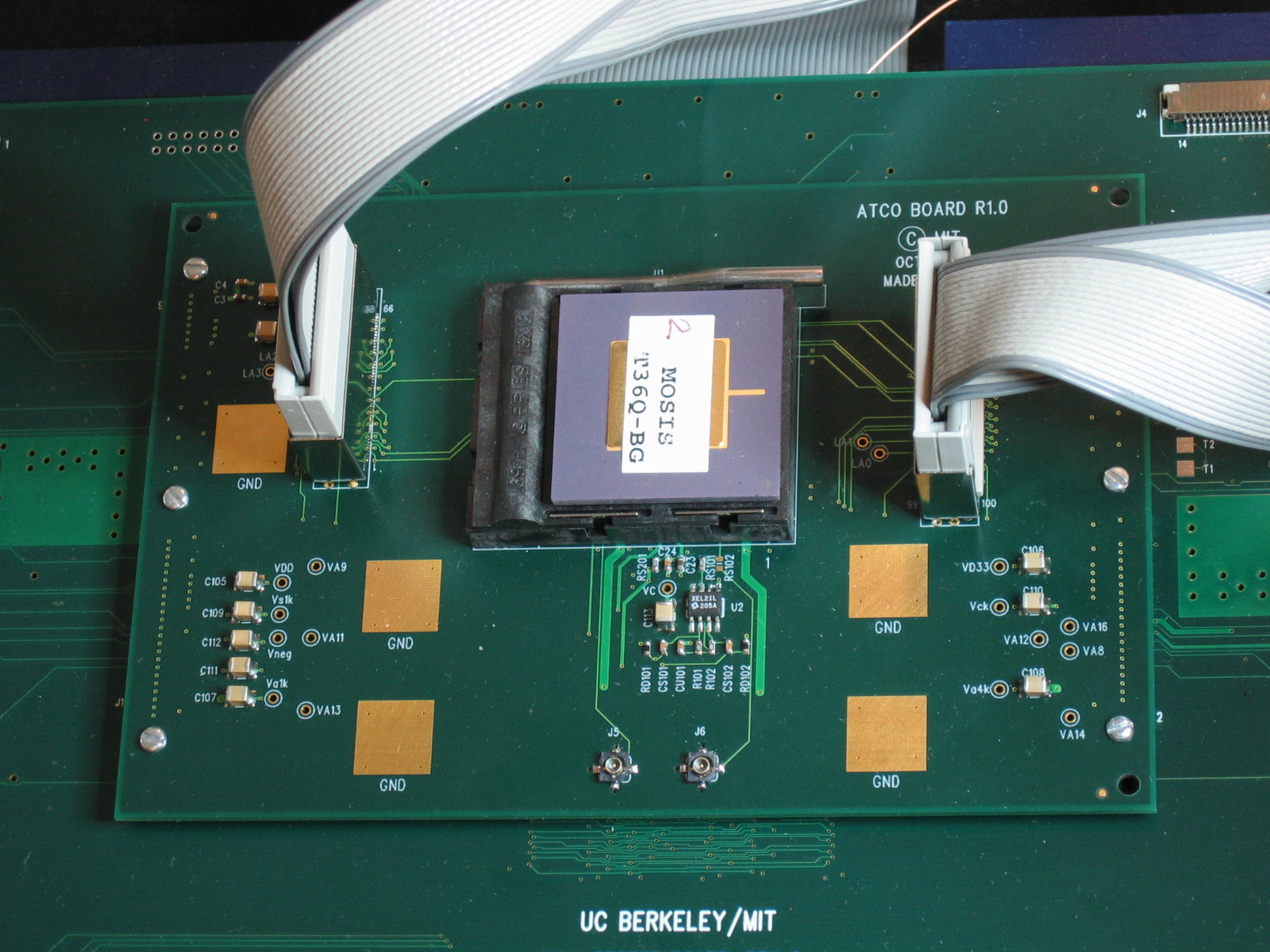
ATC0 lives on the "daughter card" shown below. You can see probe points for the various
power planes, a ZIF socket for easy swapping of chips, two connectors
to our logic analyzer, and a PECL-to-single-ended clock converter.
The daughtercard is mounted to the baseboard, our standard testing platform.